Kategorien durchsuchen
Entdecken
Fiverr Pro
Deutsch
$
USD
PCB-Design, Embedded System und Firmware-Entwicklung
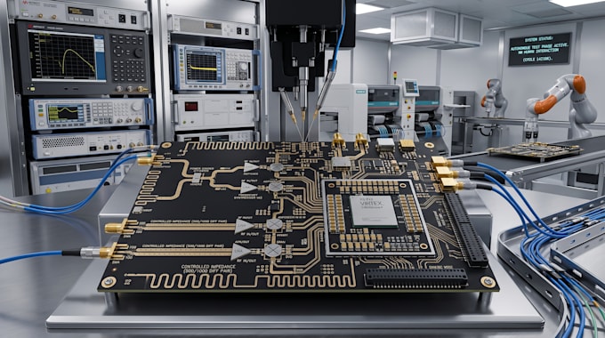
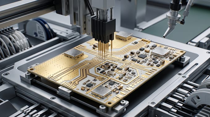
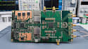
Ich spezialisiere mich auf die Entwicklung komplexer RF-PCBs und eingebetteter Hardware für drahtlose Kommunikation, IoT, industrielle Automatisierung, Luft- und Raumfahrt, medizinische Geräte, Fahrzeugtechnik, Telemetriesysteme, Module, Radar-Schnittstellen und Hochgeschwindigkeits-Digitalanwendungen.
Hochfrequenz-Elektroniksysteme erfordern weit mehr als Standard-PCB-Layout. RF-Hardware benötigt präzises elektromagnetisches Design, Impedanzkontrollierte Übertragungsleitungen, optimiertes Erdungskonzept und sorgfältig geplante Stapelaufbauten, um stabile Leistung, geringe Einfügeverluste und minimale Signalverschlechterung zu gewährleisten.
Leistungen umfassen
Was ich bereitstelle
Warum du mich wählen solltest
Bitte schreib mir
Automatische Übersetzung
Welche RF-Anwendungen unterstützt du?
Ich entwerfe RF-PCBs für Wi-Fi, Bluetooth, GNSS/GPS, LoRa, Zigbee, Module, Telemetrie, industrielle drahtlose Systeme und andere Hochfrequenzanwendungen.
Entwirfst du kontrollierte Impedanz-PCBs?
Ja. Ich setze Impedanzkontrolliertes Routing, Differentialpaare, Übertragungsleitungen und Stapelaufbauempfehlungen entsprechend den Spezifikationen deines PCB-Herstellers um.
Welche PCB-Software benutzt du?
Ich arbeite hauptsächlich mit Altium Designer und KiCad und kann auch mit bestehenden Projektdateien arbeiten.