Kategorien durchsuchen
Entdecken
Fiverr Pro
Deutsch
$
USD

Electronics Engineer , High Speed PCB and Signal Integrity
Kompetenzen
Meine Dienstleistungen

Electronics Design Engineer
LinkedIn • Selbstständig
Feb 2019 - Present • 7 yrs 8 mos
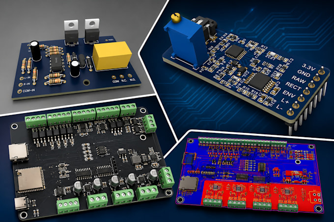
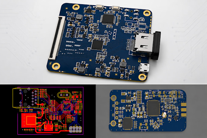
Led the hardware development and PCB layout engineering for complex high-speed communication systems, advanced IoT architectures, and multilayer industrial electronics. Key Responsibilities & Achievements: • Successfully owned the end-to-end hardware architecture, schematic capture, and layout design for 8+ layer rigid-flex boards. • Executed rigorous signal integrity (SI) and power integrity (PI) simulations to manage impedance control, cross-talk, and EMI/EMC issues on DDR4 and high-speed USB/HDMI interfaces. • Implemented strict Design for Manufacturing (DFM) and Design for Assembly (DFA) rules, reducing factory spin defects by 40% across production lines. • Utilized Altium Designer and Cadence Allegro/Sigrity daily to convert complex client technical specifications into production-ready Gerber, ODB++, and comprehensive BOM datasets.
