Kategorien durchsuchen
Entdecken
Fiverr Pro
Deutsch
$
USD
Hardware-Systemingenieur, PCB-Design, Firmware, CAD, Robotik, KI, Vision
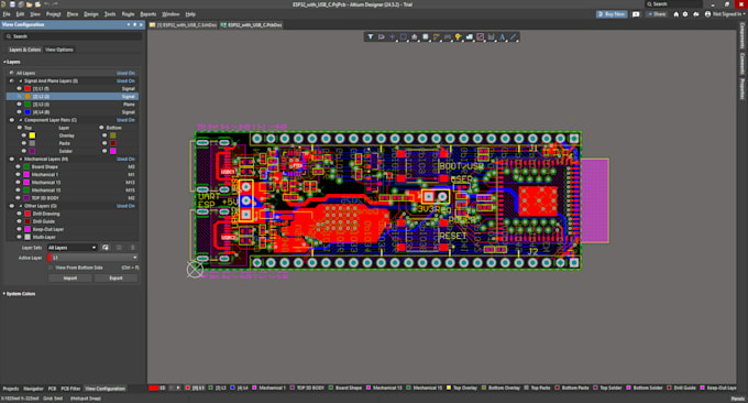
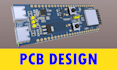
Ich entwerfe fertig für die Produktion geeignete PCBs für Embedded-Systeme, IoT-Geräte und Elektronik-Startups. Mit über 5 Jahren Erfahrung in Mechatronik und Firmware liefere ich Schaltpläne, Mehrschicht-Layouts und Fertigungsdateien, die beim ersten Mal funktionieren.
WAS ICH LIEFER:
Schaltplan mit LTspice-Simulation, PCB-Layout (2-20+ Schichten mit Impedanzkontrolle), Fertigungsdateien (Gerber, STEP, BOM), DFM-Analyse (Design for Manufacturing) und Überarbeitungsrunden.
ICH SPEZIALISIERE MICH AUF:
Mikrocontroller: STM32, ESP32, ARM Cortex | Stromversorgung, Kommunikation (USB, Ethernet, CAN, SPI, I2C, UART/USART), Sensoren
TOOLS: KiCAD, Altium Designer, LTspice
PERFEKT FÜR: Startups, Hardware-Ingenieure, Studenten, Hersteller, die IoT/Embedded-Produkte entwickeln
Schreib mir vor der Bestellung, um deine Projektanforderungen und den Zeitplan zu besprechen.


Automatische Übersetzung
Welche Angaben muss ich machen?
Mindestens eine Schaltplan- oder Schaltkreisbeschreibung. Handgezeichnet ist in Ordnung. Bevorzugt: KiCAD-Dateien, Altium-Schemata, PDFs, Breadboard-Fotos. Ich kümmere mich um die technische Umsetzung und Optimierung für die Fertigung.
Kannst du sowohl Schaltplan als auch Layout entwerfen?
Ja. Ich entwerfe vom Konzept bis zu den Fertigungsdateien. Wenn du einen Schaltplan hast, optimiere ich ihn und erstelle das Layout. Wenn du eine Schaltkreisbeschreibung hast, entwerfe ich beides von Grund auf. Komplettservice von Anfang bis Ende.
Kannst du mein bestehendes Schaltbild optimieren?
Absolut. Ich prüfe auf PCB-Layout-Beschränkungen, Bauteilplatzierung, Leiterbahnen und Signalintegrität. Viele Schaltpläne, die in der Simulation funktionieren, benötigen Optimierung für die tatsächliche Hardware-Fertigung.
Welche PCB-Tools verwendest du?
KiCAD (kostenlos/open-source) für preisbewusste Projekte, Altium Designer für professionelle Arbeiten. Ich erstelle Dateien für jede Fertigung—JLCPCB, PCBWay oder professionelle Hersteller. Gib einfach deine Präferenz an.
Übernimmst du auch Hochgeschwindigkeits-Designs?
Ja. Ich bearbeite Mehrschicht-Designs mit Impedanzkontrolle, Differentialpaaren, Masseflächenmanagement und Signalintegritätsanalyse. Ideal für USB 3.0, PCIe und Ethernet.
Kannst du die Herstellungskosten senken?
Ja. DFM-Optimierung senkt die Kosten—weniger Schichten, wenn möglich, kleinere Boards, optimierte Platzierung, Montagebereitschaft. Spart oft 30-50 % bei den Fertigungskosten im Vergleich zu unoptimierten Designs.
Was ist mit Revisionen nach der Lieferung?
Alle Pakete beinhalten Überarbeitungsrunden (1-2 je nach Stufe). Premium umfasst unbegrenzte Überarbeitungen. Für Änderungen außerhalb des ursprünglichen Umfangs berechnen wir zusätzliche Arbeit separat. Keine versteckten Kosten.
Gibst du Montageanleitungen?
Ja. Die Lieferungen umfassen BOM mit Teilenummern, Montagespezifikationen, Layer-Stackup-Dokumentation und Fertigungsdateien, die bereit für Pick-and-Place-Maschinen sind. Bei Bedarf kann ich Montagefirmen empfehlen.
Wie lange dauert das PCB-Design?
Standard: 5-7 Tage. Eilservice verfügbar (prüfe zusätzliche Services). Komplexe Designs benötigen 10-14 Tage. Ich bestätige den Zeitplan nach Absprache deines Projekts. Schnell und zuverlässig.
Funktioniert mein PCB beim ersten Prototyp?
Ich entwerfe mit Blick auf Herstellbarkeit und Funktion. Ich führe Schaltkreisüberprüfungen, DFM-Checks und Designreviews durch, um Probleme vor der Fertigung zu erkennen. Hardware ist unvorhersehbar, aber ich optimiere für Erfolg.