Kategorien durchsuchen
Entdecken
Fiverr Pro
Deutsch
$
USD
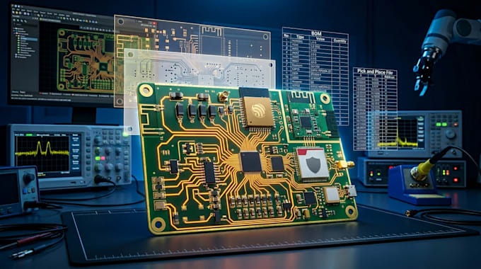
pcb design
HELLO GREAT BUYER
I'm an experienced RF PCB Design Engineer specializing in high-performance RF hardware for LoRa, GSM, GPS, Wi-Fi, Bluetooth, Zigbee, RFID, IoT, and embedded systems. Using Altium Designer, KiCad, and EasyEDA, I develop fabrication-ready PCB layouts optimized for performance and manufacturability.
WHAT I WII OFFER
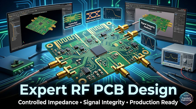
RF PCB Layout with Controlled Impedance
Why Choose Me?
I'm Let's Build Your RF Project!
Whether you're developing an RF communication device, IoT product, GPS tracker, LoRa gateway, or another wireless system, I can deliver a reliable PCB with optimized impedance control. Contact me today to discuss your project.

Dateiformat:
Gerber
•
STEP
•
BRD
•
SCH
Software:
Eagle CAD
•
EasyEDA
•
KiCad
•
LabVIEW
•
LTspice
•
Proteus
Interface:
USB
•
I2C
•
PCIe
•
Wi-Fi
•
BLE
•
BT
•
LTE
Can you design multilayer RF PCBs?
Yes. I design multilayer boards with controlled impedance and optimized RF routing.
Which RF applications do you support?
LoRa, GSM, GPS, Wi-Fi, Bluetooth, Zigbee, RFID, ESP32, STM32, and custom RF systems.