n
nicobauer_eng

Nico Bauer

@nicobauer_eng

PCB Designer '' Multilayer PCB Layout '' Manufacturing Files

Deutschland
Deutsch, Englisch, Italienisch
Einige Informationen werden in englischer Sprache angezeigt.
Über mich
I’m a professional PCB Designer specialising in PCB layout, schematic capture and circuit board routing. I help turn circuit diagrams and project requirements into clean, accurate and manufacturing-ready PCB designs. My expertise includes 2-layer and multilayer PCB layout, component placement, routing, footprint creation, DRC, DFM, Gerber files, drill files and BOM preparation. I work with Altium Designer, KiCad and EasyEDA, delivering well-organised PCB designs suitable for prototyping and production. I value accuracy, clear communication and quality results on every project.... Mehr lesen

Kompetenzen

n
nicobauer_eng
Nico Bauer
offline • 
Durchschnittliche Antwortzeit: 1 Stunde

Meine Dienstleistungen

Leiterplatten (PCB)
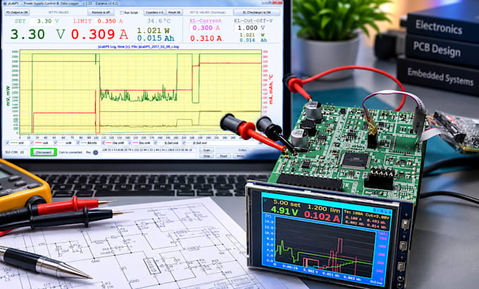
I will make hardware prototyping, schematic, pcb board designing, arduino, esp32, stm32
Leiterplatten (PCB)
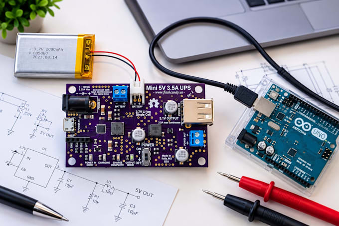
I will design pcb layout, schematic circuit, esp32 firmware in kicad, bom, gerber files

Arbeitserfahrung

Self_employed / Freelance

PCB Design Specialist

Self employed / Freelance • Selbstständig

May 2014 - Present12 yrs 4 mos

I provide professional PCB design and layout services for electronics projects, prototypes and production-ready products. My work includes schematic capture, PCB layout, component placement, PCB routing, footprint creation, multilayer board design and design optimisation. I prepare clean and organised manufacturing files, including Gerber, NC drill, BOM and pick-and-place files where required. I also perform DRC and DFM checks to help identify layout and manufacturing issues before fabrication. Experienced with Altium Designer, KiCad and EasyEDA, I focus on accurate routing, practical component placement, clear documentation and reliable PCB layouts that meet project requirements.