Kategorien durchsuchen
Deutsch
$
USD
Verbinden Sie sich mit Ihrer KI
Engineer
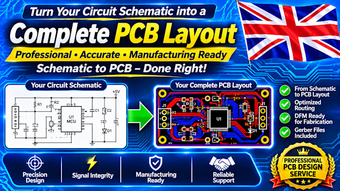
Have you finished drafting your circuit schematic but lack the time or layout software experience to design the physical board?
I will step in and convert your raw schematic diagram into a highly optimized, space-efficient, and production-ready printed circuit board.
I follow strict signal integrity rules and industry standards to ensure your physical hardware functions reliably right after assembly.
My Layout Design Framework Includes:
Supported CAD Formats: KiCad, Altium Designer, and EasyEDA (Standard/Pro).
You will receive a complete manufacturing package ready to drop straight into JLCPCB or PCBWay, along with the editable CAD project files. Bring your prototype layout to lifesend over your schematic file or netlist today to get started!
What software platforms do you use for layout design?
I build and deliver projects natively in KiCad, Altium Designer, or EasyEDA. You can specify which design environment you prefer during the onboarding stage so the final source files fit perfectly into your team's workflow.
Do you design multi-layer boards or complex physical outlines?
Yes. This package natively covers up to 4-layer designs (including inner power and ground planes) and standard or geometric board outline configurations. If your system requires highly complex high-speed multi-layer routing (6+ layers), please message me for a custom quote.
What manufacturing deliverables will I receive when the order is complete?
You will receive a production-ready ZIP archive containing Gerber files (RS-274X or X2), NC Drill files, assembly files (CPL/Pick and Place coordinates), a clean Bill of Materials (BOM), and a 3D STEP model of the board.
Will you verify that my circuit schematic logic is correct before layout?
No. This service strictly transforms your existing schematic into a physical board layout. It does not include logic verification, code debugging, or component engineering validation. Please ensure your schematic is electrically functional before ordering.
Can you adjust the layout later if my mechanical enclosure or sizing requirements change?
Minor outline revisions are completely covered within your 2 included package revisions. However, significant component repositioning or core architectural layout re-routing after the project is finished will require a custom extension order.
