Kategorien durchsuchen
Entdecken
Fiverr Pro
Deutsch
$
USD
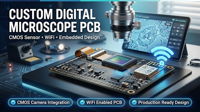
Pcb design and firmware development
HELLO AND WELCOME!
Building a high-performance digital microscope requires far more than connecting a camera module to a processor. Image quality, signal integrity, power stability, wireless connectivity, and PCB layout all play critical roles in achieving reliable performance.
I specialize in designing custom digital microscope hardware with CMOS image sensors, WiFi connectivity, and production-ready PCB layouts for commercial, medical, industrial, educational, and research applications.
What i will provide:
Why Choose Me:
Message me before placing your order so we can discuss your project requirements and choose the best package for your application!!!!


Dateiformat:
Gerber
•
STEP
•
VRML
•
3DS
Software:
Allegro
•
KiCad
•
LabVIEW
•
AutoCAD
Interface:
HDMI
•
MIPI DSI/CSI
•
I2S
•
USB
•
I2C
•
BLE
•
BT
•
LTE