Kategorien durchsuchen
Entdecken
Fiverr Pro
Deutsch
$
USD

PCB Designer
Kompetenzen
Meine Dienstleistungen

PCB designer
Jeanuvs • Vollzeit
Jan 2019 - Sep 2025 • 6 yrs 8 mos
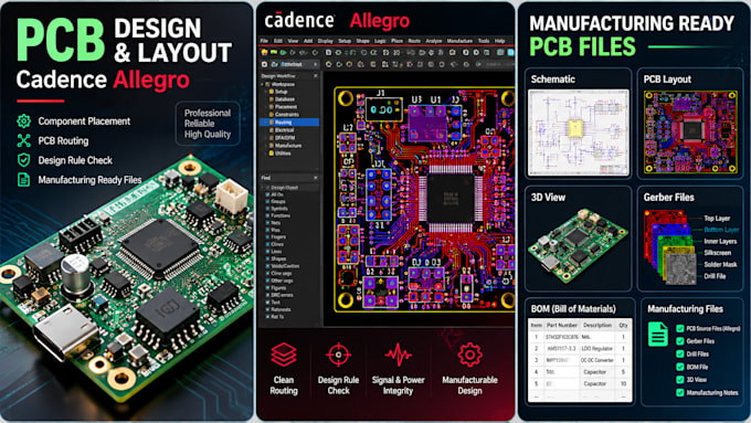
PCB Designer Jan 2019 - Sep 2025 • Specialized in PCB component and footprint creation and verification, maintaining a strong quality record across design and manufacturing workflows. • Executed DSN import, component placement, routing, and layout preparation using Cadence Allegro and OrCAD. • Performed DRC checks and design verification to identify and resolve PCB layout issues before manufacturing. • Prepared manufacturing-ready Gerber data in CAM350, including checking, editing, and merging. • Designed multilayer PCB layouts up to 10 layers independently and supported PCB designs up to 22 layers. • Managed BOM-related activities and collaborated with a 10-member team to coordinate design work, resolve issues, and support manufacturing preparation. • Maintained a strong quality record in component creation and verification, with no reported component-related errors in the designs handled.
