Kategorien durchsuchen
Entdecken
Fiverr Pro
Deutsch
$
USD

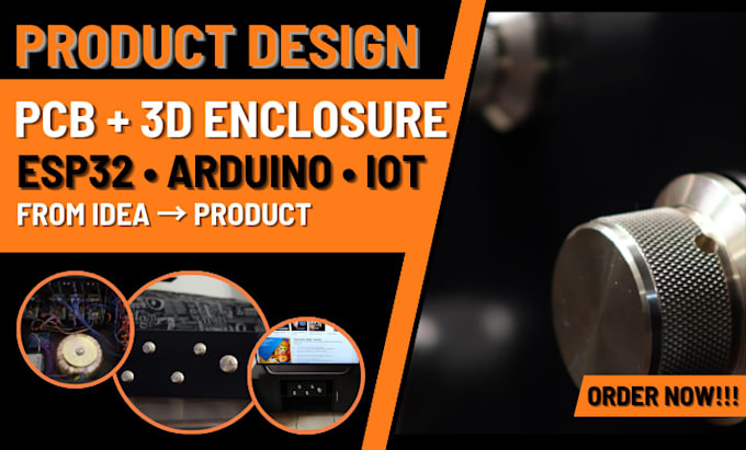
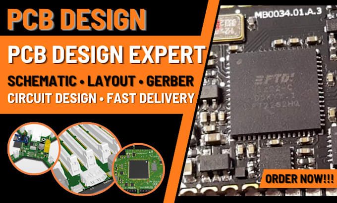
PCB Design Expert, Altium, KiCad, ESP32, Arduino And IoT
Kompetenzen
Meine Dienstleistungen
Fiverr
Freiberufler • 0 mos
Electronics Design Assistant
Aug 2025 - Aug 2025 • 0 mos
Assisted in schematic design, PCB layout, and testing of electronic systems. Supported development of embedded and IoT-based projects using microcontrollers such as Arduino and ESP32. Helped prepare manufacturing files and improve circuit performance through testing and optimization.
PCB Design Engineer
Aug 2025 - Aug 2025 • 0 mos
Design and develop PCB layouts, schematics, and circuit designs for international clients. Specialized in Altium Designer and KiCad, delivering manufacturing-ready files including Gerber, BOM, and Pick & Place. Worked on ESP32, Arduino, IoT, and embedded systems projects, ensuring optimized routing, signal integrity, and reliable performance in real-world applications.
