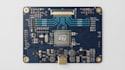
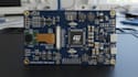
Suchst du nach einem professionellen Hochgeschwindigkeits-Kamera PCB-Layout für dein Embedded-Vision-, IoT-, Robotik- oder Elektronikprojekt?
Ich entwerfe ein sauberes, zuverlässiges und professionell organisiertes Kamera PCB-Layout mit MIPI CSI-2, ESP32, STM32 und Hochgeschwindigkeits-Signalrouting.
Meine Leistungen umfassen:
- Hochgeschwindigkeits-Kamera PCB-Layout
- MIPI CSI-2 Schnittstellenrouting
- ESP32 PCB-Layout
- STM32 PCB-Layout
- Bildsensor PCB
- Kamera-Modul Schnittstelle
- Hochgeschwindigkeits-Differentialpaarrouting
- Impedanzkontrolliertes Routing
- Mehrlagiges PCB-Layout
- Strom- und Masseflächen-Design
- Komponentenplatzierung und Optimierung
- Signalintegrität im Fokus des Routings
- Via- und Rückleitung-Optimierung
- Stromversorgungsbereich
- USB, UART, I2C, SPI und andere Schnittstellen
- Design Rule Check (DRC)
- Fertigungsbereite PCB-Dateien
Verwendbare Software:
- KiCad
- Altium Designer
- EasyEDA
Lieferumfang:
- Komplettes PCB-Layout
- Schematic-Integration
- PCB-Quell- und Projektdateien
- Gerber-Dateien
- Bohrdateien
- Stückliste (BOM)
- Pick-and-Place-Dateien bei Bedarf
- PCB-3D-Visualisierung
- Fertigungsdokumentation