Kategorien durchsuchen
Entdecken
Fiverr Pro
Deutsch
$
USD

Expert PCB Designer '' Altium and KiCad PCB Layout
Kompetenzen
Meine Dienstleistungen

PCB Design Engineer
Self employed / Freelance • Selbstständig
Dec 2011 - Present • 14 yrs 9 mos
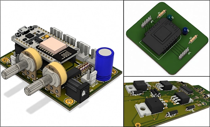
I work as a PCB Design Engineer specialising in professional schematic capture, PCB layout, component placement and routing for electronic products, prototypes and production projects. My work covers the complete PCB design process, from reviewing circuit requirements and creating or refining schematics to developing organised, manufacturing-ready board layouts. I design 2-layer, 4-layer and multilayer PCBs with careful attention to component placement, routing, power and ground planes, signal paths, trace widths, clearances and overall board organisation. I also perform design rule checks (DRC) and design for manufacturing (DFM) reviews to identify potential issues before fabrication. My PCB design services include schematic design, PCB layout, high-speed and mixed-signal routing, component footprint management, library creation, PCB stack-up planning, copper zones, vias, connectors, mounting holes and board documentation. I prepare complete manufacturing files including Gerber files, NC drill files, BOM and pick-and-place files where required. I can also review existing PCB layouts, correct design issues, optimise routing and prepare designs for professional PCB fabrication and assembly. I work primarily with Altium Designer, KiCad and EasyEDA and can work from schematics, circuit diagrams, existing PCB files, component datasheets or project requirements. My approach is focused on accurate layouts, clean documentation, manufacturability and reliable design practices.
