Einige Informationen werden in englischer Sprache angezeigt.
Über mich
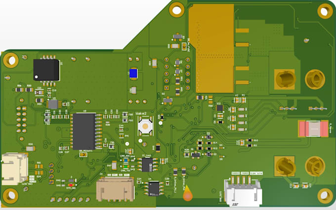
I'm a professional electronics engineer specializing in high-density, multi-layer PCB design and layout. I transform your concepts and schematics into production-ready circuit boards using industry-leading EDA tools like Altium Designer and KiCad. My designs strictly follow DFM and EMC standards to guarantee seamless manufacturing, optimal thermal performance, and signal integrity. From schematic capture to delivering final Gerber files and BOMs, I provide reliable, high-quality hardware solutions aligned to your project goals. Let's collaborate to bring your electronic products to life.... Mehr lesen