Einige Informationen werden in englischer Sprache angezeigt.
Über mich
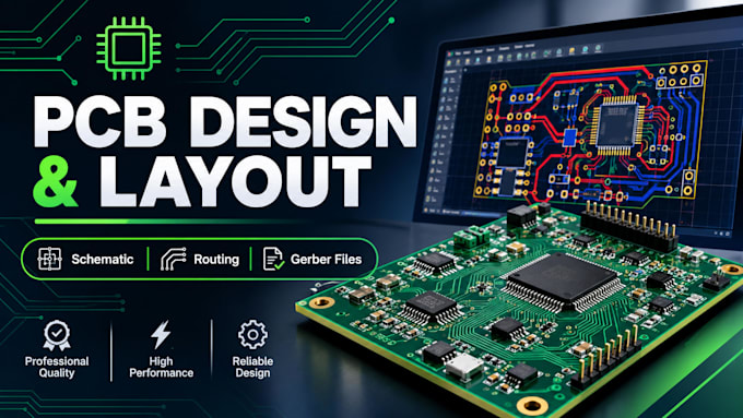
I am a professional PCB design specialist focused on creating accurate, organized and manufacturing-ready printed circuit board layouts. I provide PCB layout design, schematic capture, component placement, circuit routing, multilayer PCB design and Gerber file generation. Using tools like KiCad, EasyEDA and Altium Designer, I focus on clean routing, proper component arrangement, design rule checks and reliable project documentation. My goal is to turn your electronic project requirements into practical PCB designs with precision, quality and attention to detail.... Mehr lesen