Kategorien durchsuchen
Entdecken
Fiverr Pro
Deutsch
$
USD
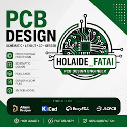
ELECTRONIC AND ELECTRICAL ENGINEER
Kompetenzen
Meine Dienstleistungen
Freelancing on Fiverr
Fiverr • Vollzeit
Apr 2025 - Present • 1 yr 3 mos
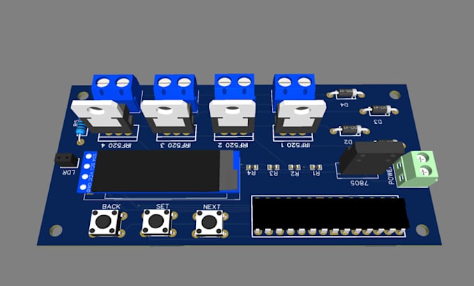
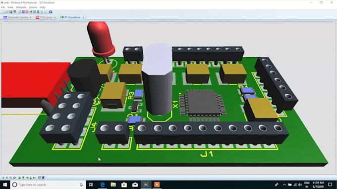
PCB Design Specialist | Offering Professional, Custom Circuit Board Solutions As a dedicated PCB (Printed Circuit Board) designer with 2 years of experience, I specialize in delivering high-quality, functional, and efficient circuit boards for a variety of applications. Whether you're working on a new product prototype, a modification to an existing design, or a fully functional production-ready board, I can provide professional assistance that meets your specific requirements. Key Skills and Expertise: Schematic Design: Translating your ideas into functional circuit diagrams. PCB Layout: Designing compact, reliable, and manufacturable PCB layouts using industry-standard tools like Eagle, KiCad, or Altium Designer. Component Selection: Recommending the best components for performance, cost-effectiveness, and availability. Design for Manufacturability (DFM): Ensuring that the PCB design is easy to produce with minimal cost and complexity. Signal Integrity Analysis: Addressing issues related to high-speed signals, EMI, and PCB trace routing to ensure optimal performance. Gerber File Generation: Providing all the necessary files for manufacturing, including Gerber files, BOM (Bill of Materials), and pick-and-place files. Prototype Support: Assisting with PCB prototyping and troubleshooting to ensure that your design works as expected. Why Choose Me? High-Quality Design: I prioritize creating PCBs that are not only functional but also optimized for cost and manufacturability. Attention to Detail: I review every aspect of the design to ensure reliability and performance. Fast Turnaround: I understand deadlines are crucial, so I ensure timely delivery without compromising on quality. Clear Communication: I keep you informed throughout the design process, ensuring your requirements are met and any concerns are addressed promptly. Previous Work & Projects: Designed PCBs for consumer electronics, medical devices, IoT products, and automotive applications.
