h
hansottoqy

Hans Klunder

@hansottoqy

Electronic engineer, pcb designer and firmware expert

Deutschland
Deutsch, Englisch
Einige Informationen werden in englischer Sprache angezeigt.
Über mich
Hi, I’m Hans Klünder, a professional electronics and PCB design engineer specializing in end to end hardware development solutions. I help individuals, startups, and businesses turn ideas into fully functional electronic products through PCB design, circuit development, embedded systems, and advanced engineering solutions. My expertise covers PCB schematic design, multilayer PCB layout, IoT and embedded systems development (ESP32, Arduino, STM32), PCB optimization for manufacturing, and high performance industrial circuit design including power electronics and RF systems.... Mehr lesen

Kompetenzen

h
hansottoqy
Hans Klunder
offline • 

Meine Dienstleistungen

Leiterplatten (PCB)
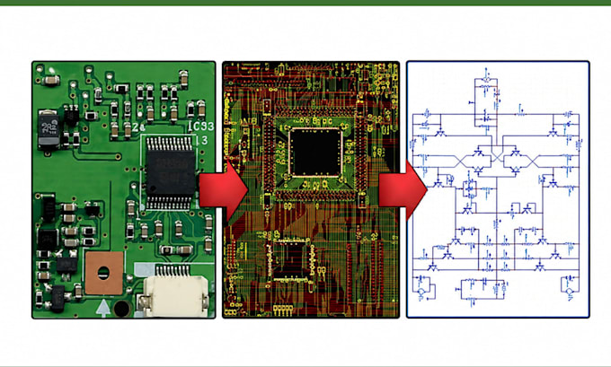
I will design pcb schematic and layout for esp32 arduino stm32 with gerber and bom
Leiterplatten (PCB)
I will review and fix pcb design, schematic and layout issues

Arbeitserfahrung

ZEISS_Group

Software engineer

ZEISS Group

Feb 2024 - Sep 20247 mos

I worked on the software update for drivers for devices for Extreme Ultraviolet Lithography.

Freelance

Software Engineer

Freelance

Nov 2019 - Jul 20208 mos

I wrote embedded firmware for devices that test high voltage batteries. The firmware drives relais and converters configuring contacts, resistors, voltage and current and measuring the resulting values.