Kategorien durchsuchen
Entdecken
Fiverr Pro
Deutsch
$
USD

PCB Design Engineer, Multilayer PCB, Embedded Systems and IoT Hardware Expert
Kompetenzen
Meine Dienstleistungen
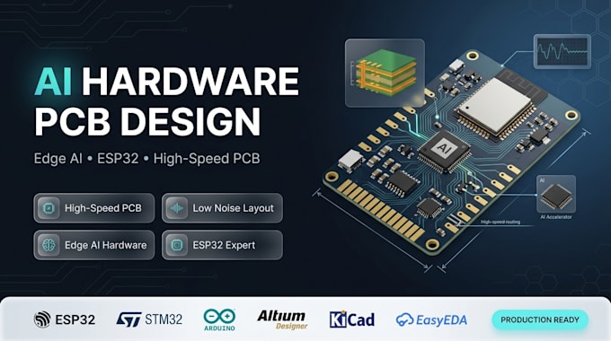
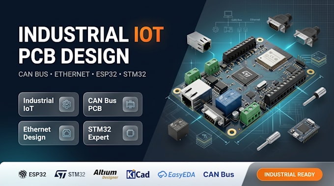
PCB Design Engineer
Upwork • Freiberufler
Sep 2025 - Present • 10 mos
As a freelance PCB Design Engineer, I specialize in designing reliable and manufacturing-ready printed circuit boards for embedded systems, IoT devices, industrial automation, robotics, and consumer electronics. My responsibilities include schematic capture, PCB layout, multilayer routing, signal integrity optimization, component placement, and Design for Manufacturing (DFM). I work with platforms such as Arduino, ESP32, STM32, and Raspberry Pi to develop efficient hardware solutions tailored to client requirements. Key Achievements 1. Successfully completed numerous PCB design projects for startups, makers, and electronics companies. 2. Designed professional 2-layer and multilayer PCBs with optimized signal routing and low-noise performance. 3. Delivered complete manufacturing packages, including Gerber files, BOM, Pick-and-Place, and fabrication outputs. 4. Assisted clients with PCB cloning, redesign, reverse engineering, and prototype optimization. 5. Improved product reliability through proper grounding, EMI reduction, power integrity, and DFM best practices. 6. Maintained excellent client communication, resulting in repeat business and long-term collaborations.
