f
fawas_exp

William Kensing

@fawas_exp

PCB Design Engineer, Schematic Design, PCB Layout Specialist, 3d printing

Großbritannien
Englisch, Spanisch, Deutsch, Japanisch
Einige Informationen werden in englischer Sprache angezeigt.
Über mich
I am William Kensington, a dedicated PCB (Printed Circuit Board) specialist with a strong focus on delivering precise, reliable, and production-ready designs. I have hands-on experience in schematic design, PCB layout, and optimization for performance and manufacturability. My approach combines technical accuracy with attention to detail, ensuring every project meets industry standards and client expectations. Whether you need a simple circuit board or a complex multilayer design, I am committed to providing high-quality results, clear communication, and fast turnaround... Mehr lesen

Kompetenzen

f
fawas_exp
William Kensing
offline • 
Durchschnittliche Antwortzeit: 1 Stunde

Meine Dienstleistungen

Leiterplatten (PCB)
I will do pcb design, pcb layout, reverse engineering, schematic design, gerber files
Leiterplatten (PCB)
I will do professional pcb design, circuit schematic, pcb layout in kicad and esp32

Arbeitserfahrung

Fiverr

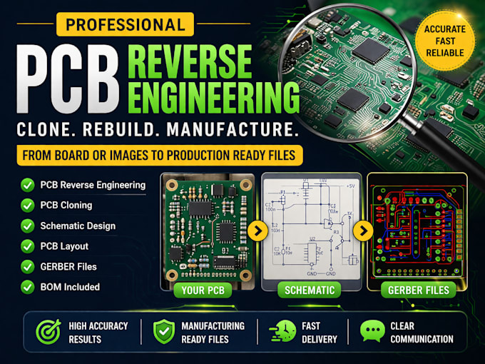
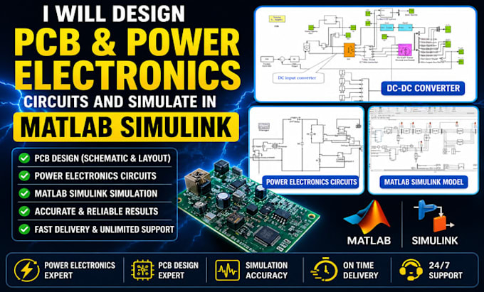
Freelance PCB Designer & 3D Printing Specialist

Fiverr • Freiberufler

Jun 2024 - Present2 yrs

Designed and developed custom PCB schematics and layouts for various electronic projects Created efficient and production-ready PCB designs using tools like KiCad / Eagle / Altium Developed 3D models for prototyping and product design using Fusion 360 / Blender Prepared and optimized files for 3D printing (STL, slicing, print settings) Worked on multiple personal and client-based projects, ensuring high-quality results Focused on accuracy, functionality, and clean design standards