Kategorien durchsuchen
Entdecken
Fiverr Pro
Deutsch
$
USD
PCB, RF, Antenna, IoT and Circuit Design Engineer
SERVICE I OFFER
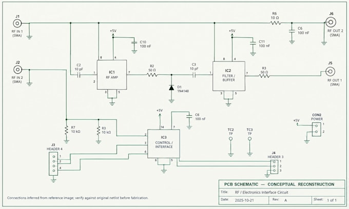
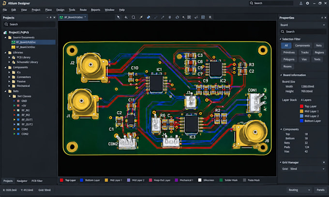
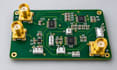
Custom RF PCB design and wireless PCB layout for Wi-Fi, Bluetooth, LoRa, GPS and other high frequency radio designs. I place the RF section, route controlled impedance lines and keep the ground return clean, so your radio has the best chance of working as intended on the first build.
WHAT YOU WILL GET
Manufacturer ready Gerber files with a layer stackup that matches your fabricator's capabilities. I work from your schematic, module datasheets and any reference layout, and I tell you early if something in the design looks risky.
WHY CHOOSE ME
A layout built for low RF loss: short matched traces, proper grounding, isolation from noisy power and digital sections, and attention to EMI. Clear communication and honest expectations: I will not promise a specific range or certification result, since that depends on your antenna, enclosure and testing.
DELIVERABLES
Gerber and drill files, impedance control and stackup notes, PCB layout source files, a PDF of the layout and a short design note.
Send me your schematic and requirements, and I will confirm scope before you order. Message me first for complex or multi radio boards.
Which radios and frequencies do you work with?
Wi-Fi, Bluetooth, LoRa, GPS and similar sub-6 GHz designs. Tell me the module and band before ordering and I will confirm it fits.
Can you guarantee my range or certification?
No. Range and certification depend on your antenna, enclosure and testing. I design the layout to give the radio its best chance.
Do I need to send a schematic?
Yes, a schematic or module reference design is the starting point. If you only have an idea, see my schematic and layout Gig.
Which files do I get?
Gerber and drill files, stackup and impedance notes, layout source files and a PDF, depending on the package.
Do you design the antenna too?
Antenna design and tuning is a separate Gig. This one places and routes the RF section around your chosen antenna.