Kategorien durchsuchen
Entdecken
Fiverr Pro
Deutsch
$
USD
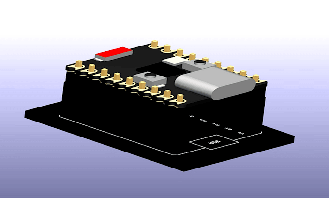
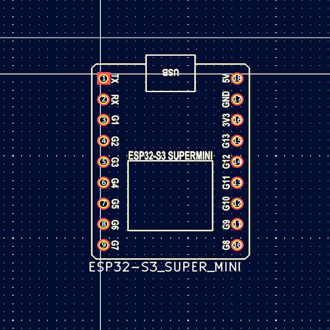
Professional PCB Kicad designer
Are you struggling to turn your smart device or wearable idea into a working PCB?
Many projects fail due to poor circuit design, messy layouts, power issues, signal instability, or boards that cannot be manufactured.
These problems delay development and increase costs.
I will solve this by creating professional KiCad PCB designs for smart devices and wearable electronics.
I focus on compact, efficient, and reliable layouts for modern portable technology.
What I design:
Benefits:
Files delivered:
Lets turn your idea into a clean, reliable, and manufacturing-ready PCB.
Message me now to get started.


Can I request revisions if needed?
Yes, I offer revisions to ensure your PCB design meets your exact requirements.
What files will I receive after completion?
You will get KiCad files, Gerber files, schematic PDF, BOM, Pick & Place, and drill files.
What software do you use for PCB design?
I mainly use KiCad for design and also support Altium, EasyEDA, and Eagle if required.
Can you design PCB for wearable and IoT devices?
Yes, I specialize in KiCad PCB designs for smart devices, wearables, and IoT projects.
What do you need to start my PCB design?
I need your circuit idea, schematic (if available), component list, or a reference image/drawing.