Kategorien durchsuchen
Entdecken
Fiverr Pro
Deutsch
$
USD
I convert your ideas into real world ptroducts
Hi,
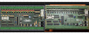
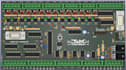
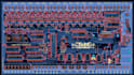
I provide PCB reverse engineering, PCB layout, and schematic recreation services for existing circuit boards, along with the manufacturing files required for PCB production.
I am an experienced PCB designer with 10+ years of experience in PCB layouts and PCB reverse engineering. I work with KiCad, Altium Designer, and EasyEDA.
My PCB reverse engineering services include:
I can also work with custom-shaped PCBs according to your requirements.
Please contact me before placing an order and share clear images or details of your PCB so I can review the project and provide the right package.
I look forward to working with you!
Can you reverse engineer multi-layer PCBs?
Yes, I can work with single-layer, double-layer, and multi-layer PCBs. Please contact me for complex or high-layer-count boards.
What files will I receive?
Depending on the selected package, I can provide Gerber files, PCB source files, schematic, BOM, and Centroid/Pick & Place files.
Can you identify components from the PCB?
I can identify components and footprints where their markings and available information are sufficient.
Can you recreate a PCB with a custom shape?
I can recreate custom-shaped PCBs based on the original board dimensions and requirements.
Can you modify the PCB after reverse engineering?
I can make PCB layout modifications and design changes based on your requirements.


